Chromium Complexes Of Graphene
Patent Status
| Country | Type | Number | Dated | Case |
| United States Of America | Issued Patent | 9,266,738 | 02/23/2016 | 2011-255 |
Full Description
Background
Graphene based electronic devices have the potential in achieving high performance in electronic and semiconductor applications because of its unique electronic properties that are complemented by its excellent mechanical and thermal properties. To adequately realize the potential of graphene as an electronic material there is a need to modifying graphene without much perturbation of its conjugated p -electron clouds. Attempts to covalently modify graphene to introduce bandgap have resulted in the hybridization of the sp2 carbon atoms to sp3 leading to serious disturbances of the p -electron clouds.
Current Invention
Inventors led by Prof. Robert Haddon at UCR have developed an innovative, patented system and method for milder covalent modification of graphene without much perturbation of the structural integrity of the sp2 hybridized carbon atoms. The invention provides a general system and method for hexahapto (h 6) complexation of graphene with group 6 transition metals to various extended periodic p -electron systems where the primary h 6 ligand is solely a carbon material.
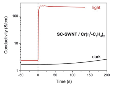
Evolution of the conductivity of semiconducting SWNT films in the presence of room light and in the dark.
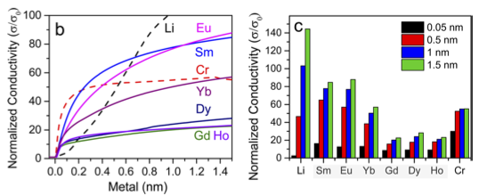
Effect of metal deposition on electrical conductivity of semiconducting SWNT films
Advantages
The significance and benefits of this invention are:
Suggested uses
The invention has broad applicability in:
Related Inventions
Please see other inventions by Prof. Robert Haddon
Related Materials
- Organometallic chemistry of extended periodic p-electron systems: hexahapto-chromium complexes of graphene and single-walled carbon nanotubes
- Photochemical generation of bis-hexahapto chromium interconnects between the graphene surfaces of single-walled carbon nanotubes
- Effect of Lanthanide Metal Complexation on the Properties and Electronic Structure of Single-Walled Carbon Nanotube Films
- Effect of constructive rehybridization on transverse conductivity of aligned single-walled carbon nanotube films
Contact
- Venkata S. Krishnamurty
- venkata.krishnamurty@ucr.edu
- tel: View Phone Number.

Other Information
Keywords
Carbon nanotubes, Single Walled Carbon Nanotubes, SWNT, Organometallic functionalization, Conductivity, Interconnects, Chromium, Carbon nanotube film, lanthanides, Optical properties, Optoelectronics