Solution Processing Of Transition Metal Dichalcogenide Thin Films
Patent Status
| Country | Type | Number | Dated | Case |
| United States Of America | Issued Patent | 9,991,390 | 06/05/2018 | 2014-807 |
Full Description
Background
Molybdenum Disulfide (MoS2) belongs to a class of materials called Transition Metal Dichalcogenides (TMD). TMDs have the chemical formula MX2 where M is a transition metal such as Molybdenum, Tungsten, etc. and X is from the chalcogen group. After graphene, MoS2 is the next 2-dimensional material being researched for new device applications given its strong optical and electronic properties. Methods for producing MoS2 include micromechanical exfoliation, solvent exfoliation and intercalation. The challenge with these top-down approaches is that their size renders them unsuitable for electronic applications. Other processing methods may leave undesirable carbon residue.
Current Invention
Prof. Cengiz Ozkan and his research team at UCR have developed and synthesized atomically thin, large area MoS2 sheets. The patented technology synthesizes MoS2 sheets on SiO2/Si substrates at wafer scale by thermolysis of spin coated, (NH42)2MoS4 films. They have also used this method to prepare WS2 (Tungsten Disulfide) and hybrid MoS2-WS2 thin layers.
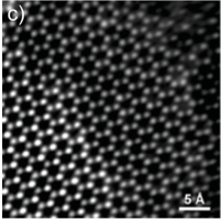
High-angle, annular dark-field scanning, Transmission Electron Microscopy image showing tri-, bi- and monolayer MoS2 (from left to right).
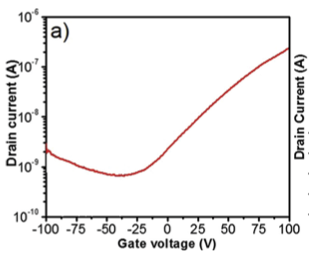
Plot of drain current versus gate voltage for fabricated FET showing electron transport. The on/off ratio for this device is 300.
Advantages
The benefits of their technology are:
Suggested uses
- Field effect transistors, high-efficiency switching and logic circuits
- Photodetectorrs
- Solar cells
- Chemical sensors
- Supercapacitor electrodes
- Next generation Valleytronics – e.g., quantum computing and qubits.
Testing
To evaluate, they fabricated Field Effect Transistors (FET) on SiO2/Si substrate with Ti/Au contacts. FETs show electric mobilities of 0.1 sq. cm per Volt per second.
Related Materials
Contact
- Venkata S. Krishnamurty
- venkata.krishnamurty@ucr.edu
- tel: View Phone Number.

Other Information
Keywords
Transition Metal Dichalcogenides, Monolayer MoS2, Molybdenum Disulfide, 2 dimensional nanosheets, Photoluminescence, Photodetectors, Semiconductors, Optoelectronics, Chemical sensors, Solar cells, Electrodes, Valleytronics, Logic circuits, High efficiency on/off switches