Stacked-Via Metal Tube And Wall For Noise Isolation At Transistor And Circuit Levels In Ics
Full Description
Background
Advanced analog/mixed signal (AMX) and radio frequency (RF) integrated circuity are increasingly challenged by noise/crosstalk (noise therafter). Traditional in-substrate noise-isolation approaches cannot address in-BEOL (backend-of-the-line) global flying noises, which emerges as the main noise for large, complex chips at advanced technology nodes. Existing in-BEOL shielding solutions require process modification to BEOL, incompatible to standard CMOS.
Invention
Prof. Albert Wang has invented a novel, in-BEOL stacked-via metal tube/wall structures to effectively suppress global flying noises, which can be readily implemented at both transistor and circuit levels in foundry CMOS by LAYOUT designs, demonstrating up to 17 dB noise reduction in 38 GHz RF SPDT fabricated in foundry 45nm SOI CMOS.
Images
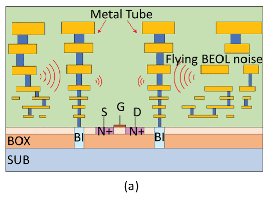
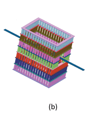
(a) A cross-section view of the new in-BEOL stacked-via metal tube global flying crosstalk suppression structure in silicon-on insulator (SOI). (b) 3D diagram of in-BEOL metal tube.
Advantages
- 100% CMOS process compatibility
- Easy layout design in any foundry CMOS
- Transistor/device and circuit block levels
- Global flying noise isolation
- Ideal for fabless IC design houses
Suggested uses
Global flying noise isolation/suppression for any AMX/RF chips, e.g.,:
- 5G/6G RF IC chips
- Automotive system on a chip (SoC) sensitive to electromagnetic compatibility (EMC)
- Implantable medical electronics
Related Materials
Patent Status
Patent Pending
Contact
- Venkata S. Krishnamurty
- venkata.krishnamurty@ucr.edu
- tel: View Phone Number.

Other Information
Keywords
stacked via, metal tube, metal wall, global flying noise, crosstalk, back end of the line, BEOL, CMOS, SOI, IC, integrated chip