Strain Gated Molybdenum Disulfide Field Effect Transistor With Edge Contacts
Patent Status
| Country | Type | Number | Dated | Case |
| United States Of America | Issued Patent | 10,263,107 | 04/16/2019 | 2017-489 |
Full Description
Background
Strain engineering is a process that can improve the performance of transistors by modifying the materials to enhance electron mobility. Silicon transistors benefit from strain engineering, but their 3D structure limits the amount of strain they can withstand. Transition metal dichalcogenides (TMDCs), which are only a few atoms thick, tolerate much higher levels of strain - making them good candidates for strain engineering.
Technology
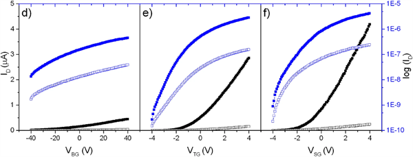
UCR team led by Prof. Cengiz Ozkan has demonstrated a novel strain-gate molybdenum disulfide (MoS2) field effect transistor (FET) by applying a silicon nitride stress liner - an industry compatible process used to improve performance of silicon transistors. The team found that increasing tensile strain in the bilayer MoS2 decreased the conduction band gap thereby significantly increasing the electron mobility and the electrical performance of the MoS2 transistors.
Image

Gate transfer plots (d to f) with the linear axis on the left in black color and the log axis on the right in blue. The curves with filled markers correspond to a VDS bias of 1V; those with empty markers have VDS of 100 mV.
Advantages
- Industry compatible method for improving the performance of MoS2 transistors for use in logic devices.
- 58% increase in electron mobility and 46% increase in on-current magnitude, i.e., the amount of electrical current that can flow through.
- One-dimensional edge contacts achieves a higher yield of working transistors with improved performance repeatability.
- Resistant to defects often found on natural MoS2 crystals.
- The method does not require external strain inducing equipment and could potentially be applied to other TMDCs to enhance their electrical properties.
Suggested uses
Scaling performance of transistors
Inventor Information
Please review all inventions by Prof. Ozkan and his team at UCR.
Related Materials
Contact
- Venkata S. Krishnamurty
- venkata.krishnamurty@ucr.edu
- tel: View Phone Number.
Other Information
Keywords
strain engineering, transition metal dichalcogenides, MoS2, Molybdenum disulfide, field effect transistors, FET, electron mobility, silicon nitride, edge contacts, band gap
