De Novo Graphene-Based Electrodes, Ultracapacitors, Batteries, Biosensors, Photovoltaic Cells, Hierarchical And Layered -
Patent Status
| Country | Type | Number | Dated | Case |
| United States Of America | Issued Patent | 10,287,677 | 05/14/2019 | 2011-520 |
Full Description
Background
Graphene is a one atom thick, honeycomb lattice of carbon atoms with outstanding electrical and physical properties and is exploited for several applications including solar cells and energy storage. Large area synthesis of high-quality graphene is vital for its widespread application. Carbon nanotubes (CNT), given their unique properties, have been extensively investigated. However, it is difficult to assemble graphene and CNTs with controllable architecture at the nanoscale.
Current Invention
UCR research team led by Prof. Cengiz Ozkan have developed a patented method for the fabrication of Pillared Graphene Nanostructures (PGN) comprised of stacked CNTs on large area, graphene layers. The Chemical Vapor Deposition (CVD) growth process uses either acetylene of methane as the carbon source to fabricate, in situ, a large area PGN with controlled architecture.

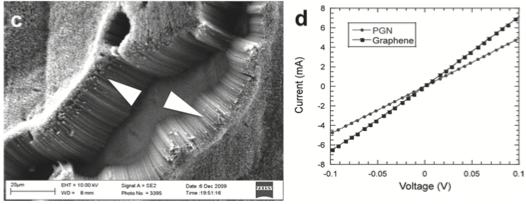
Figure c is a Scanning electron micrograph of a scratched PGN surface displaying the uniformity of the CNT pillars on the graphene layer. Figure d shows the good ohmic contact between the CNT pillars and the graphene film.
Advantages
The benefits of their fabrication method are:
Suggested uses
- Energy storage – especially dielectric capacitors and electro-chemical supercapacitors.
- Photovoltaics or solar cells.
- Nanoelectronics.
- Biosensors.
Related Materials
Contact
- Venkata S. Krishnamurty
- venkata.krishnamurty@ucr.edu
- tel: View Phone Number.
Other Information
Keywords
Graphene, Carbon Nanotube, Pillared Graphene Nanostructures, Capacitors, Supercapacitors, Photovoltaics, Solar energy, Nanoelectronics, Biosensor
