Tip-enhanced Raman Spectroscopy Probes for use with AFM
Technology Description
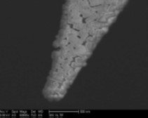
Offered here is a new method to cost-effectively batch produce consistent, high-quality, high-yield Tip-enhanced Raman Spectroscopy (TERS) Probes. Using a bath process, SiO2 AFM probes are selectively coated with a dense size-ordered-layer of engineered nanoparticles, providing a high resolution & high sensitivity probe tip that exhibits reproducible enhancement from one tip to the next. Unlike current state-of-the-art (evaporative coating, wire-etching or top-down construction) the current tip is both reliable and predictable in its performance. Leveraging this new method for TERS Probe production, the full potential for TERS imaging should be realized at cost effective prices.
The given method improves upon current approaches in several aspects:
1) The process uses superior materials. As opposed to bulk metal wires or deposited metal films, the method herein uses size and shape controllable nanoparticles. These particles are single crystalline, nearly-atomically flat and are advantageous over deposited or etched materials which have shapes that are uncontrollable on the nanoscale, are rough and polycrystalline.
2) Because the fabrication process is independent of the size or shape of the nanoparticles used, this method succeeds in engineering the desired size and shape of nanoparticle for a given probe, allowing precise tuning of the antenna’s performance to meet experimental criteria.
3) The combination of high quality materials and tunability has led to reproducible enhancement factors in the range of 108-109 at a wavelength of 785 nm. This compares to most etched metal or evaporation coated tips which are generally in the 106-107 range.
4) This is a batch process. Many of the existing fabrication techniques have single-tip throughput. Thus far, this method has demonstrated up to 10 simultaneously fabricated tips, made in 3-5 hours, with a greater than 80% yield. It should be noted that fabricating 50 or 100 tips would add little to no extra time to the process.
Applications
Experiments to date using a silicon-tipped Atomic Force Microscope, enhanced with the above method, have yielded exceptional data at the nm scale. There are several markets today which would benefit from broader availability of TERS, the largest of which is the semiconductor industry. TERS can give information about dopants, stress/strain, material composition, crystal orientation, and other properties of semiconductor and solid state devices that are unobservable with other current techniques.
There are many interesting biological questions that can be addressed with TERS as well. There has been a publication suggesting TERS can be used to sequence DNA. It may also be useful for looking at cell membrane composition and dynamics, as well as many other potential biological applications.
The TERS tips developed under this research have proven easy enough to use, that anyone currently operating an AFM should be able to perform TERS successfully. They should also be affordable enough to become consumables in the price range of research labs.
This technology should help bring TERS technology to the broader market.
Patent Status
| Country | Type | Number | Dated | Case |
| United States Of America | Issued Patent | 10,012,674 | 07/03/2018 | 2016-056 |
Contact
- University of California, San Diego Office of Innovation and Commercialization
- innovation@ucsd.edu
- tel: View Phone Number.

Other Information
Keywords
atomic force, microscopy, probes, raman spectroscopy probes, material, material fabrication