Ultrafast Welding of Ceramics
Full Description
Background
Joining ceramic substrates is challenging and traditional methods using heat often result in cracks. Ultrafast lasers have been successfully used in joining glass but their use in ceramics has been limited because ceramics are not transparent. Use of continuous wave lasers have been explored but these require high power and preheating to avoid damaging the ceramic substrates. A commonly used method, diffusion bonding, requires heating the entire ceramic assembly to high temperatures for many hours. Diffusion bonding is costly and only works with small number of ceramics. There is a need for an efficient, low temperature method to join ceramics.
Technology
Researchers from the University of California campuses in Riverside and San Diego have developed an all ceramic, hermetically sealed package for encapsulating electronics. The developed technology uses disparate transparent polycrystalline ceramics and is sealed by ultrafast lasers. The laser directly joins the disparate surfaces, protecting the electronic device from damage while ensuring a high-quality seal. The inventors strategically considered both the optical properties of the polycrystalline ceramics and the laser parameters such as exposure time, number of pulses, and pulse duration - femto second versus pico second. Two different concepts have been identified:
- Transparent ceramics for hermetic encapsulation; and,
- Diffuse ceramics to demonstrate joining of simple geometries.
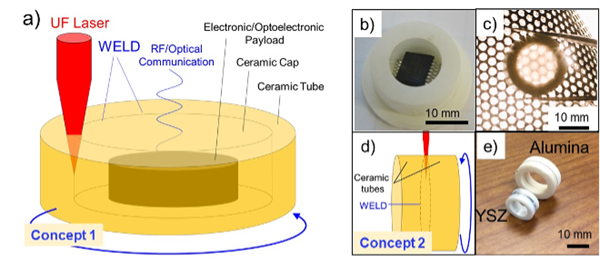
(a) Schematic illustration of concept 1 above; (b) picture of a sample electronic payload (an integrated chip) placed inside a ceramic tube; (c) picture of a successfully welded assembly of concept 1 - the background pattern (pitch 3.5mm is visible through a transparent ceramic cap); (d) schematic of concept 2 for welding simple ceramic geometries; and, (e) picture of a successfully welded assembly of alumina and ytria-stabilized zirconia (YSZ).
Advantages
- The method is versatile for a wide variety of ceramic materials and for a diversity of device geometries.
- Vacuum testing of the assemblies showed the ability to hold a high vacuum with a leak rate that is one order of magnitude better than the requirement for hermetic seals. The assembly satisfies the modern specifications and standards for bio-implantable electronics, military, and space applications.
- Compared to traditional diffusion bonding which uses 1000-Watt high temperature furnaces, the current technology uses an ultrafast laser of 50 Watts (maximum power) and consumes on the order of 25 Watt-hour.
- Opens the possibility for creating more complex and intricate ceramic designs.
Applications
- For use as a packaging material for biomedical implants like pacemakers and for future medical technologies like optogenetics.
- Electronic and opto-electronic packaging.
- Ceramic packaging of sensors.
Patent Status
| Country | Type | Number | Dated | Case |
| United States Of America | Issued Patent | 12,384,728 | 08/12/2025 | 2015-938 |
Related Materials
- E.H. Penilla, et al., “Ultrafast laser welding of ceramics”, Science, 365, pp. 803–808, 2019 - 08/23/2019
- Biocompatibility and thermal profile of transparent nanocrystalline yttria-stabilized-zirconia calvarium prosthesis.
Other Information
- Please see press coverage on the Window to the Brain implant which provided the inspiration for the laser joining of transparent ceramics.
- Please visit the Center for the Synthesis of Advanced Materials for Biomedical Applications (C-SAMBA) at UCR.
- Please review other medical device inventions by Prof. Aguilar and his team at UCR.
Contact
- Venkata S. Krishnamurty
- venkata.krishnamurty@ucr.edu
- tel: View Phone Number.

Other Information
Keywords
laser sealing, transparent, polycrystalline, implant