DCRAM: A VLSI Circuit For Mixed Memory Storage And Polymorphic Logic Computing
Background
The present von Neumann paradigm for stored-program computers involves a significant amount of information transfer between the central processing unit (CPU) and memory. As program instructions and data must share time on the memory bus, a natural bottleneck occurs, wasting a good deal of CPU capacity while awaiting the next instruction. To overcome this bottleneck, a new approach is presented here that couples computing and memory storage onto the same device, gaining substantial new efficiencies and offering the first practical variation on computer design in several decades.
Technology Description
Described here is a new solution based on memcapacitor technology referred to as DCRAM (Dynamic Computing Random Access Memory) which effectively combines memory storage and computing onto the same substrate. Fig. 1 shows the concept demonstrated with memcapacitors. Early results show the possibility of overcoming the problem associated with the intrinsically dissipative memristor technology, as the memcapacitors consume much less power and are capable of storing information on a more reliable basis. Moreover, it can be implemented in VLSI using similar technological solutions for standard DRAMs allowing for large scale low-cost production, very low power consumption and mixed mode operation for memory storage and polymorphic logic computing on the same physical platform.
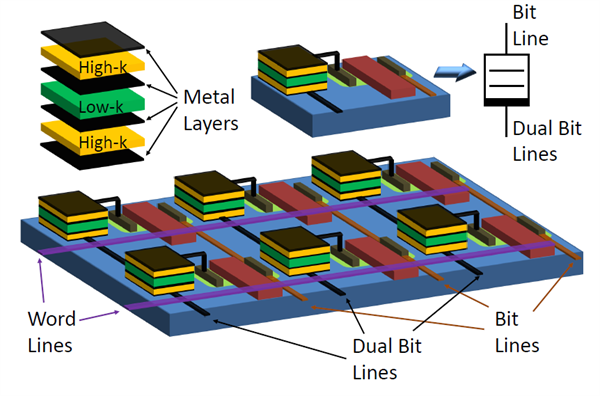
Fig.1 Configuration of a 6-bit memory cluster
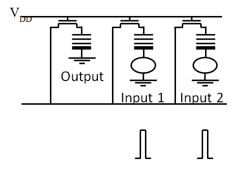
Fig. 2 Configuration of three memory cells for polymorphic computing
Applications
The write, read and refresh processes can be performed in a similar way as for DRAMs using a configuration composed of word line (WL) and double bit line (bit line (BL) and dual bit line (DBL).
Using DCRAMs it is also possible to make computation directly inside the platform. It can be reached simply by working with two, three or more memory cells with common WL. In figure 2, shown above, the configuration of three memory cells is sketched. In this configuration, the BLs of three cells have the sense amplifiers (SAs) temporarily disconnected and they are connected together to a floating common line. The output of the memcapacitor is initially set to a certain state and voltage pulses with different amplitudes are successively applied at the DBLs. The global current response of the three memory cells will depend on the internal states of the memcapacitors.
Advantages
The DRRAM concept is not limited to the specific circuit realizations shown in Figs 1 and 2, shown above, or particular realization of memcapacitors. Modifications of the above mentioned architectures could involve a variety of additional circuit components optimizing desired operations. For example, the same memcapacitor could be used to store Input and Output values. In this case, the circuit from Fig. 2 reduces to a circuit of 2 memcapacitors coupled to a traditional capacitor.
State Of Development
Intellectual Property Info
Related Materials
Patent Status
| Country | Type | Number | Dated | Case |
| United States Of America | Issued Patent | 9,570,140 | 02/14/2017 | 2013-158 |
Contact
- University of California, San Diego Office of Innovation and Commercialization
- innovation@ucsd.edu
- tel: View Phone Number.